Service Benefits
|
|
Tekwiss USA provides semi custom products of moderate complexity
at extremely low cost using Mixed Signal Gate Array (MSGA)
technology. Our engineering team will define, design and verify
your gate array solution as well as deliver the complete
packaged and tested product in an accelerated timeframe.
The new MSGA
technology provides the following great benefits:
-
Lowest cost: Cuts development costs by more than 50%,
compared with full custom ASIC method
-
Fastest development: Full product development cycles of
4-6 months are usual
-
Lowest risk: Proven chip reliability
-
Highest integration: Extremely small footprint allows
significant reduction in size/weight of our customers end
products.
|
|
Features
|
|
MSGA supports
following features: |
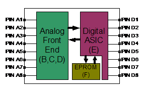
Block Diagram
|
|
Vcc (power supply) |
1 6 V
|
|
Chip size |
1.7 mm2
|
|
Input/Output cells |
16 |
|
Digital 2-input
standard gates |
1100 |
|
EPROM cells |
32 |
|
Analog P- and
N-MOS transistors |
800 |
|
Resistors |
470 |
|
Capacitors |
200 |
|
Metal layer plus
via |
2 |
|
Maximum clock rate |
20 MHz |
|
 |
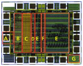
Layout
|
_________________________________
|
A |
Input/Output
cells |
|
B |
Analog part |
|
C |
Capacitors |
|
D |
Level shifter |
|
E |
Digital part |
|
F |
EPROM cells |
|
G |
Protection
diodes |
|
 |
Product Description
|
|
MSGA technology offers different predefined active and passive
components which can be interconnected by two customized metal
layers. This significantly reduces both development cost and
time to market for analog and digital design products of
moderate complexity.
The low threshold
voltage makes MSGA-based chips very suitable for use in
battery-powered products requiring low voltage and minimal power
consumption. Furthermore, the extremely small footprint makes
these chips perfect for applications in small sensors.
MSGA-based
chips are particularly attractive for a variety of applications
in measurement technology, building control and medical
technology
for complete integration of electronic hardware components of a
circuit board into an ASIC. |
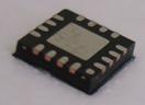
Package
|
Terminal Description
|
Picture view
|
 |
 |
Dimensions
|
|
Type |
QFN16 |
|
Length |
4 mm |
|
Width |
4 mm |
|
Height |
0.9 mm |
|
Cost
|
|
|
While manufacturing cost remains fixed, development cost depends
on the complexity of the design. Manufacturing cost for wafer
prototypes and for complete chips are as follows: |
|
Multi Project
Wafer Service |
|
Prototype
integration incl. 10 chips |
$2,500 |
|
Delivery of small
lot |
On request |
|
Chip cost incl.
packaging and test |
|
Chip cost
(depending on volume) |
$0.50-3.00 |
|
|
|
Solutions
|
The complete turn-key
custom product services include:
-
Complete ASIC
specification
-
Algorithm
development and modeling
-
Architecture
design
-
Gate Array design
(RTL coding, verification, synthesis and layout)
-
Gate Array
prototyping
-
Prototype
characterization
-
Development of
test plan
-
Coordination of
manufacturing
|
|
|
|
|